Apple ][+ Repair
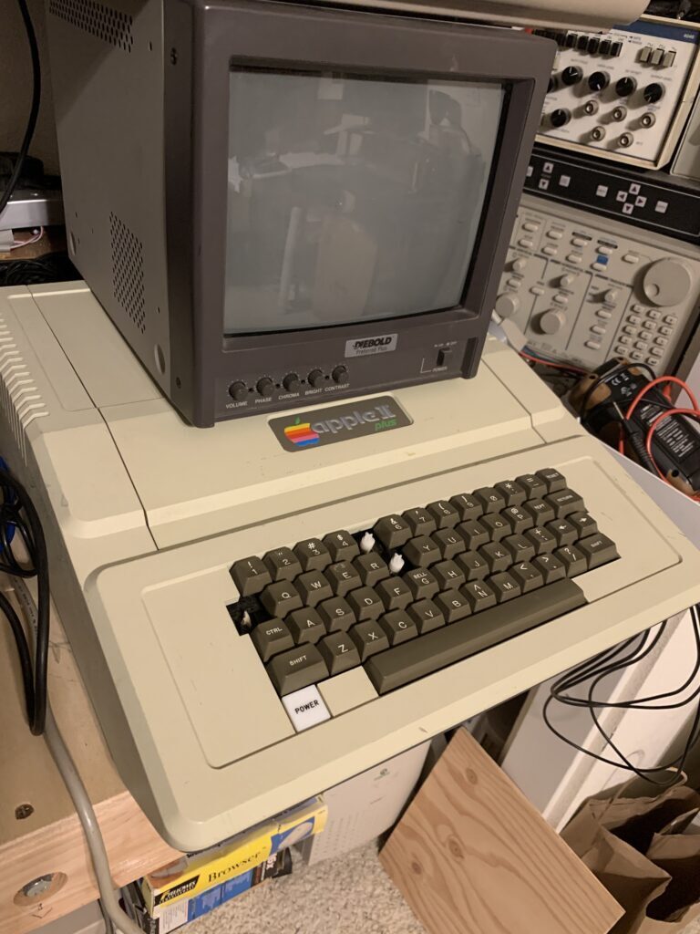
I acquired this Apple ][+ in a retro tech lot that I didn’t anticipate buying when I met the seller for the Asus P2B-D motherboard I’d agreed to buy.
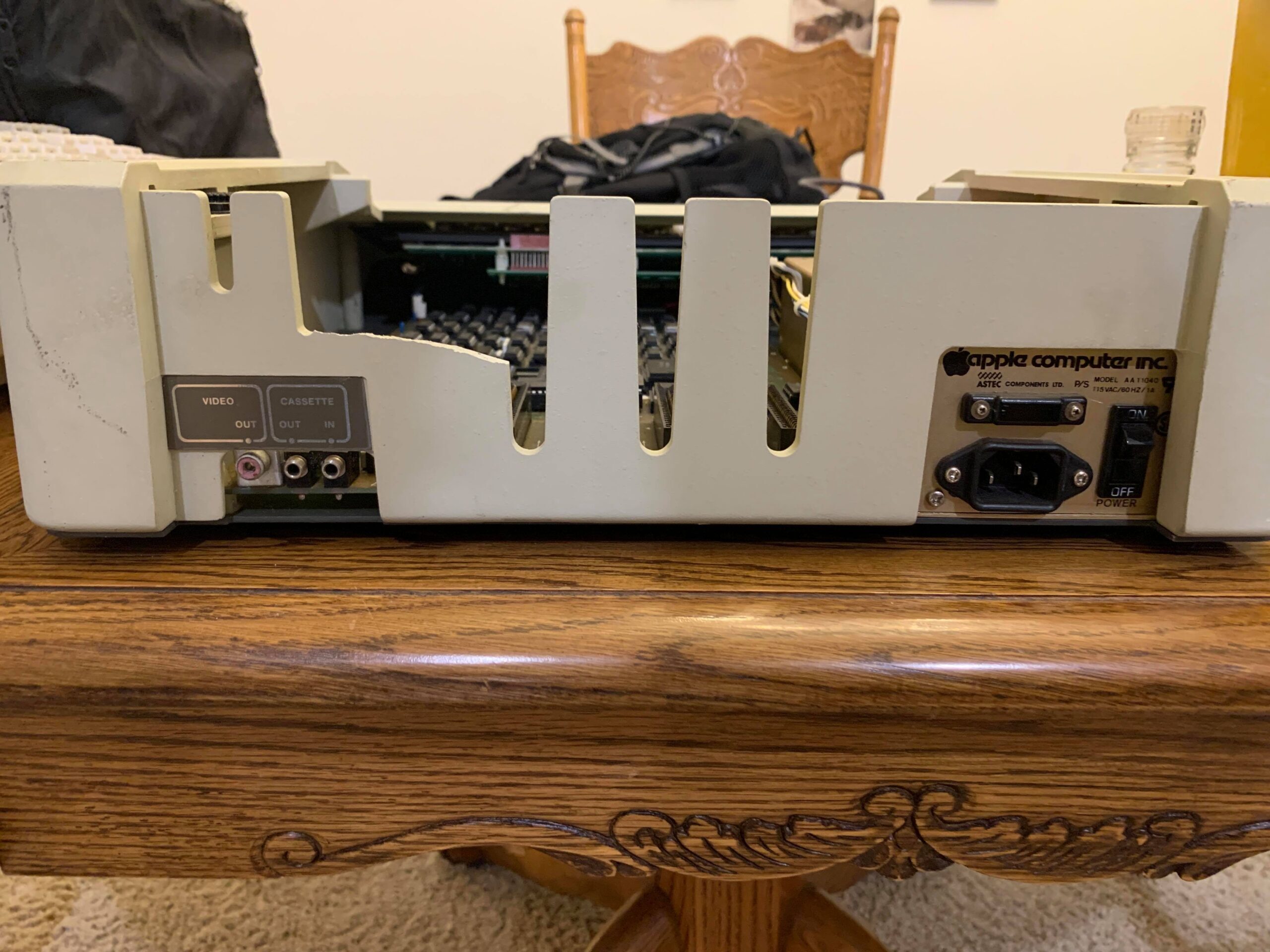
It had obviously been abused by a previous owner. Note the missing keycaps, broken key stem for what should be the escape key, missing lid & ROM ICs, broken IC sockets, and broken plastic on the rear.
Despite the damage, I was happy to have a 6502 based system other than my NES & Nintendo VS arcade machine PCB.
Besides, if the system was already in working order, it wouldn’t be much of a project! It kept me busy throughout the pandemic in 2020.


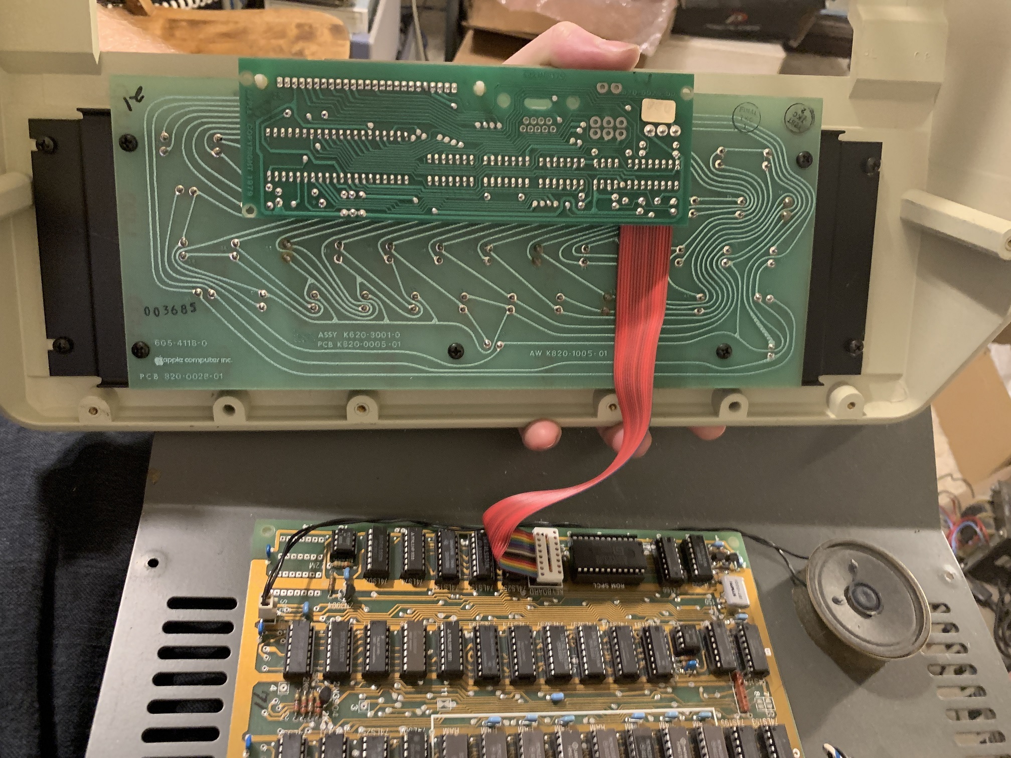
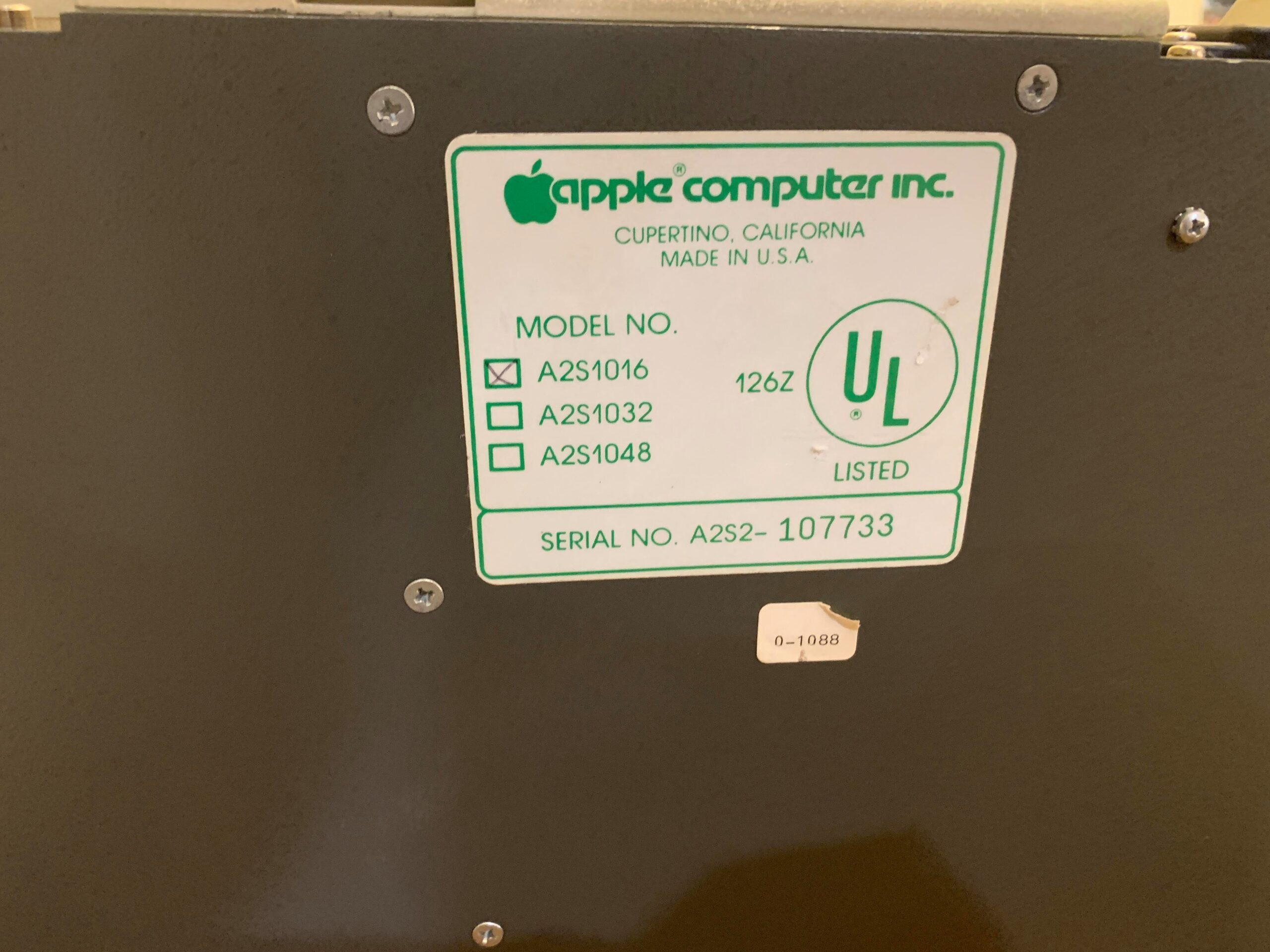
According to the sticker on the bottom of the chassis, this system was originally shipped with 16KB of RAM, and sometime during its life the system was upgraded to a full 48KB of onboard memory. On the upper left corner of the motherboard is (what I’m assuming) a date code, which indicates that it was produced in the 30th week of 1980. The motherboard is revision 7.
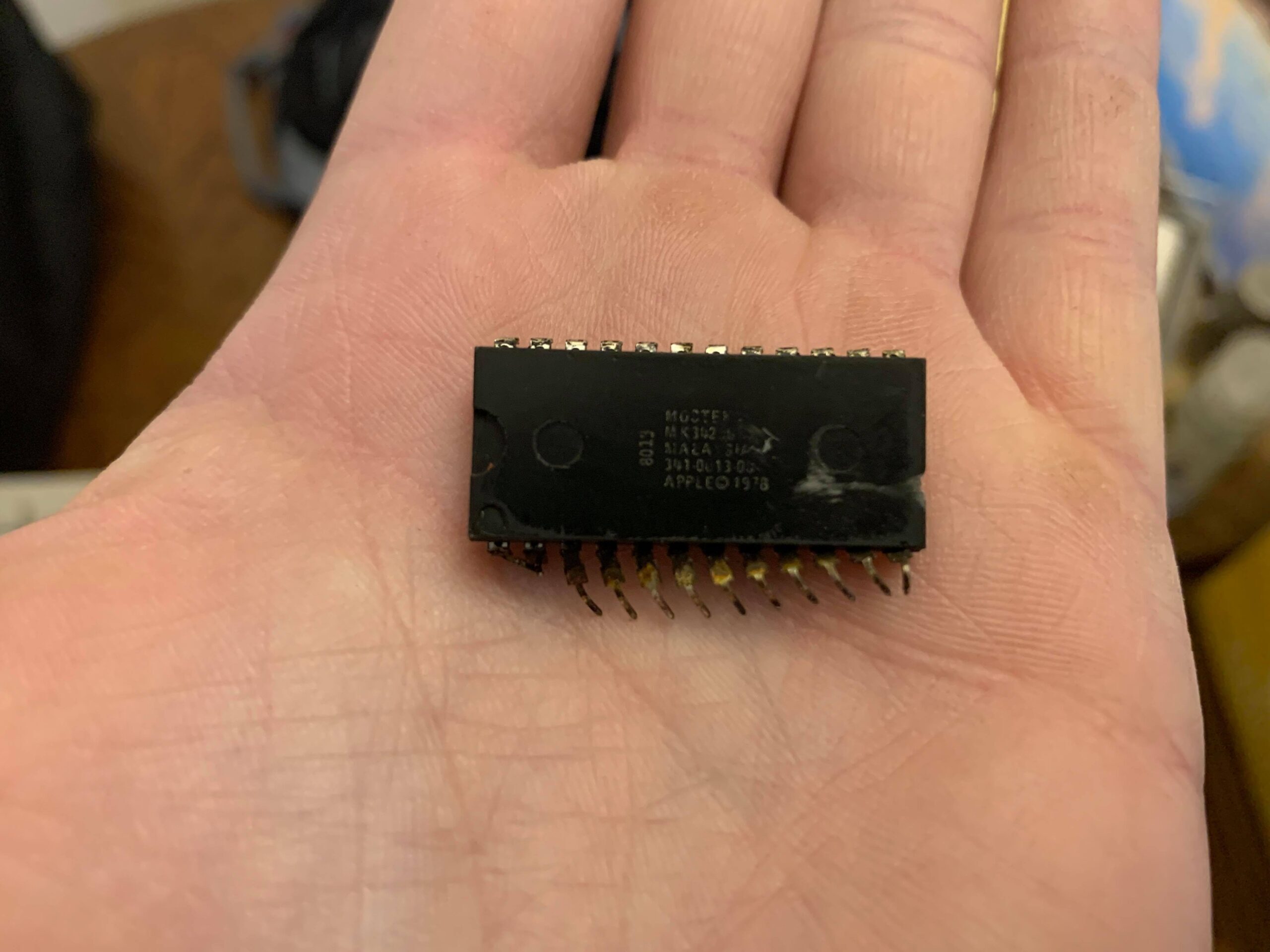
Due to a very damaged ROM IC with another one missing altogether, I decided to pull all the ROM ICs and come up with temporary solution. Taking a close look at the schematic, I thought a quick approach to replacing the individual ROM ICs was to instead use one large flash EEPROM. My implementation actually uses a 128KB flash EEPROM and wastes most of its space. The benefits are a small component count and ease of wiring.
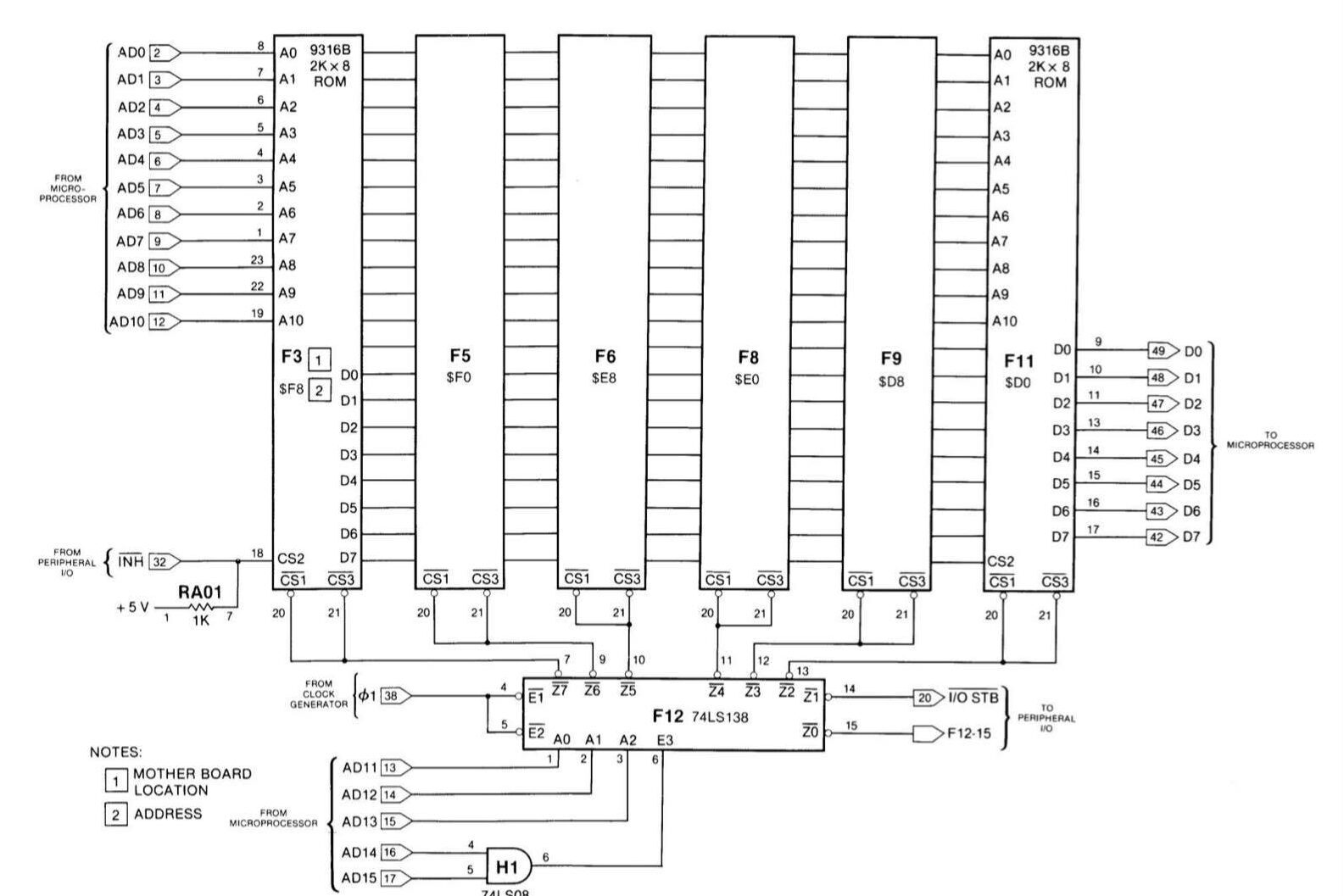
The 74LS138 3-to-8 decoder takes address lines 11 through 13 as inputs. The decoder is only enabled when the ϕ1 clock is LOW and both address lines 14 & 15 are HIGH. It asserts only one of its 8 active low ROM select lines at a time as its output according to the binary sequence of address lines 11 through 13. This creates different blocks of memory for the 6 ROM ICs: $D000-$D7FF, $D800-$DFFF, … $F800-$FFFF as well as select lines for I/O.
For a detailed representation of this, see this table:
| AD15-AD11 | Address Range | Output |
| 00XXX | N/A | All Unasserted (HIGH) |
| 01XXX | N/A | All Unasserted (HIGH) |
| 10XXX | N/A | All Unasserted (HIGH) |
| 11000 | $C000-$C7FF | ~Z0 Asserted (LOW) |
| 11001 | $C800-$CFFF | ~Z1 Asserted (LOW) |
| 11010 | $D000-$D7FF | ~Z2 Asserted (LOW) |
| … | … | … |
| 11111 | $F800-$FFFF | ~Z7 Asserted (LOW) |
The ROM ICs have 11 address lines worth of data, so there are 211 = 2048 bytes of data in each ROM IC. Six of these make 12KB of data. The quick approach I took to connecting this large flash EEPROM, in place of the smaller ROM ICs, was by taking each of the six original ROM IC select lines and using them as additional address inputs on the EEPROM. The system requires that the EEPROM be enabled only when the following conditions are met concurrently: ~INH is unasserted, and the address range for any of the six ROM ICs is accessed. For that, I used two 74 series ICs: a triple 3-input NAND IC (74LS10) and an OR IC (74LS32). You can see the logic in the schematic below.

When the system is accessing an address outside the range for the ROM, the inputs to the two 3-input NAND gates on the left are all HIGH, so their outputs are LOW, making the OR gate output LOW. Thus the output of the last NAND gate will be HIGH, which disables the ROM.
Anytime the system asserts the ~INH signal, the output of the last NAND gate will be HIGH, which disables the ROM.
Finally, when the system is accessing an address within the range for the ROM and the ~INH signal in unasserted, one of the corresponding ~Zx outputs from the 3-to-8 decoder will go LOW. The output for the corresponding NAND gate will go HIGH, which makes the OR gate output HIGH. The output of the final NAND gate will then be LOW, which enables the ROM.
The trade off of this technique, which uses very little hardware, is that the internal organization of the ROM data for the flash EEPROM becomes a little convoluted.
Here is the internal flash EEPROM memory map that the design requires:
| System Address Range | EEPROM A16-A11 | EEPROM Address Range |
| $D000-$D7FF | 111110 | $1F000-$1F7FF |
| $D800-$DFFF | 111101 | $1E800-$1EFFF |
| $E000-$E7FF | 111011 | $1D800-$1DFFF |
| $E800-$EFFF | 110111 | $1B800-$1BFFF |
| $F000-$F7FF | 101111 | $17800-$17FFF |
| $F800-$FFFF | 011111 | $0F800-$0FFFF |
I wrote a small Python script to take the six ROM files and arrange them into one file with the correct organization. Outside of valid ROM addresses, the script pads the file with $FF. This fills the unused addresses with known data, a requirement for programming this particular EEPROM.
new_file = open("apple_II+_128k_rom.bin", "wb")
i = 0
while i < 131072:
    if i == 0xF800:
        input_rom = open("F8.bin", "rb")
        while i < (0xF800 + 0x00800):
            new_file.write(input_rom.read(1))
            i += 1
        input_rom.close()
    if i == 0x17800:
        input_rom = open("F0.bin", "rb")
        while i < (0x17800 + 0x00800):
            new_file.write(input_rom.read(1))
            i += 1
        input_rom.close()
    if i == 0x1B800:
        input_rom = open("E8.bin", "rb")
        while i < (0x1B800 + 0x00800):
            new_file.write(input_rom.read(1))
            i += 1
        input_rom.close()
    if i == 0x1D800:
        input_rom = open("E0.bin", "rb")
        while i < (0x1D800 + 0x00800):
            new_file.write(input_rom.read(1))
            i += 1
        input_rom.close()
    if i == 0x1E800:
        input_rom = open("D8.bin", "rb")
        while i < (0x1E800 + 0x00800):
            new_file.write(input_rom.read(1))
            i += 1
        input_rom.close()
    if i == 0x1F000:
        input_rom = open("D0.bin", "rb")
        while i < (0x1F000 + 0x00800):
            new_file.write(input_rom.read(1))
            i += 1
        input_rom.close()
    new_file.write(bytes([0xFF]))
    i += 1
new_file.close()
After burning the file to the EEPROM, I built the circuit on a breadboard and connected it to the system.

To test the power supply prior to energizing the rest of the system, I disconnected the power supply from the motherboard and switched the power supply on to measure output voltages. The voltages seemed close enough, or at least safe enough (5.0V, 11.7V, -4.7, & -10.9V), so I reconnected the power supply and powered on the system. The result was a static image on the display but no power light. After power cycling the system, the results were slightly improved (static image on the display, but with a power light).
After another power cycle, my monitor began to hum loudly, so I shut the system off. I turned it on yet again to see the original result, with no power light. Then, against my better judgement, I decided to power cycle the system really fast to see if the power light would turn on. Unfortunately, this time the system would not turn on at all. No light, nothing on the screen. I disconnected the power supply from the system and measured its output voltages. No voltage was present.
Suspecting that I’d blown a fuse in the power supply, I carefully drilled out the rivets and opened it up. Indeed the 2.75A fuse was spent. I placed an order for replacement fuses and capacitors. Although the original capacitors seemed fine visually, I decided to replace them while the power supply was opened up.
While waiting for the parts to arrive, I looked over everything I had done and realized I’d made a mistake. The error isn’t shown above, but my original Python script was incorrect. I had mistakenly thought that the ~Zx outputs of the 3-to-8 decoder were active high even though I had drawn them correctly on the schematic. The system’s CPU never received valid ROM data, only $FF. Oops! I corrected my mistake. Once the order arrived, I replaced the power supply capacitors and installed a new fuse.
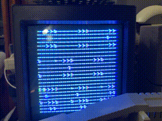
I switched the system on, and the fuse blew immediately in a quick but bright flash. Using my multimeter in diode test mode, I found that half of the bridge rectifier had shorted out. After replacing the failed rectifier and fuse (good thing I ordered multiple!), I once again switched the system on resulting in a similar static image on the display. I wiggled the video connector, and the display changed to this alternating pattern:
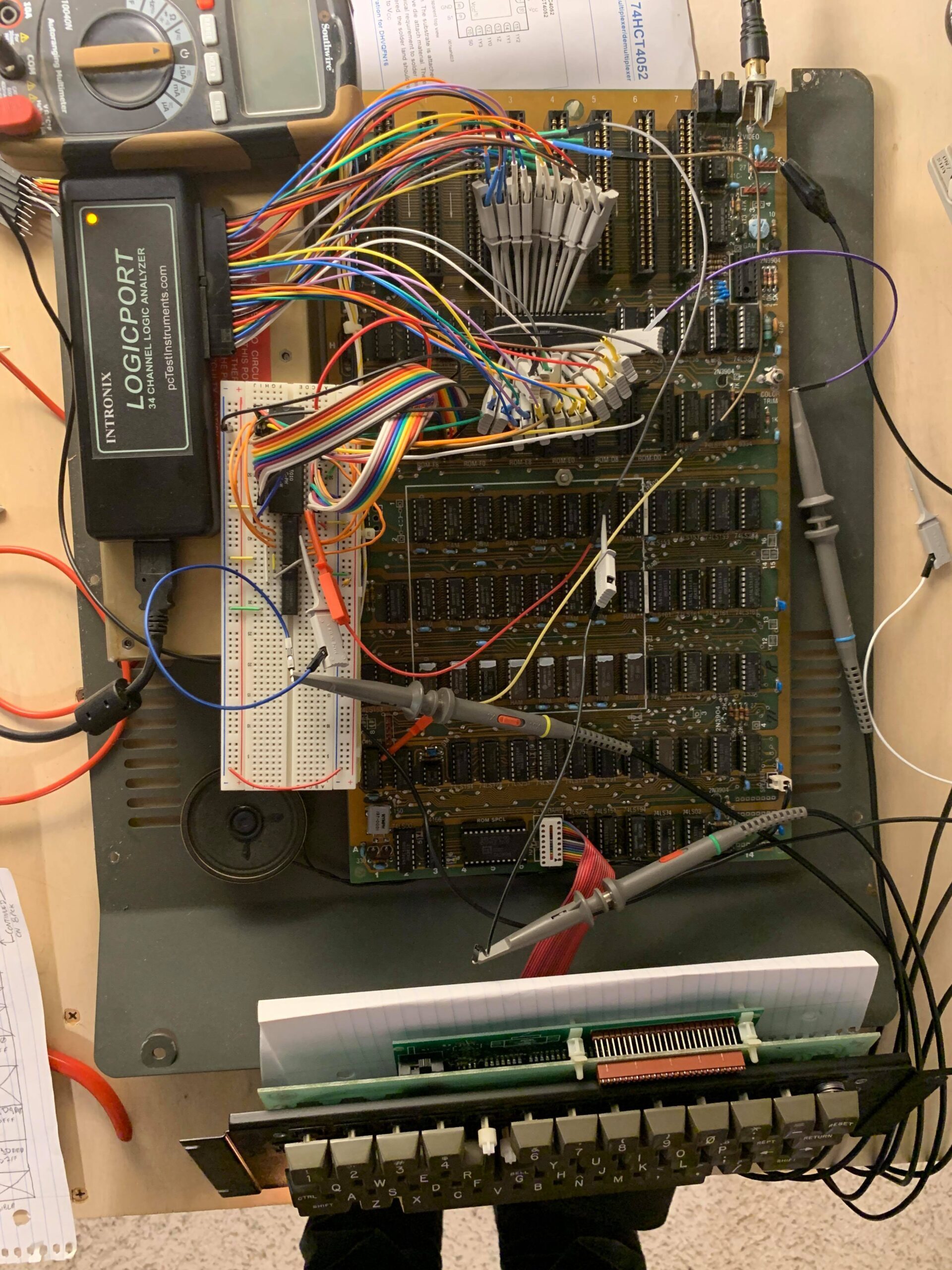
Next, I decided to connect a logic analyzer to the address and data busses to observe system behavior.
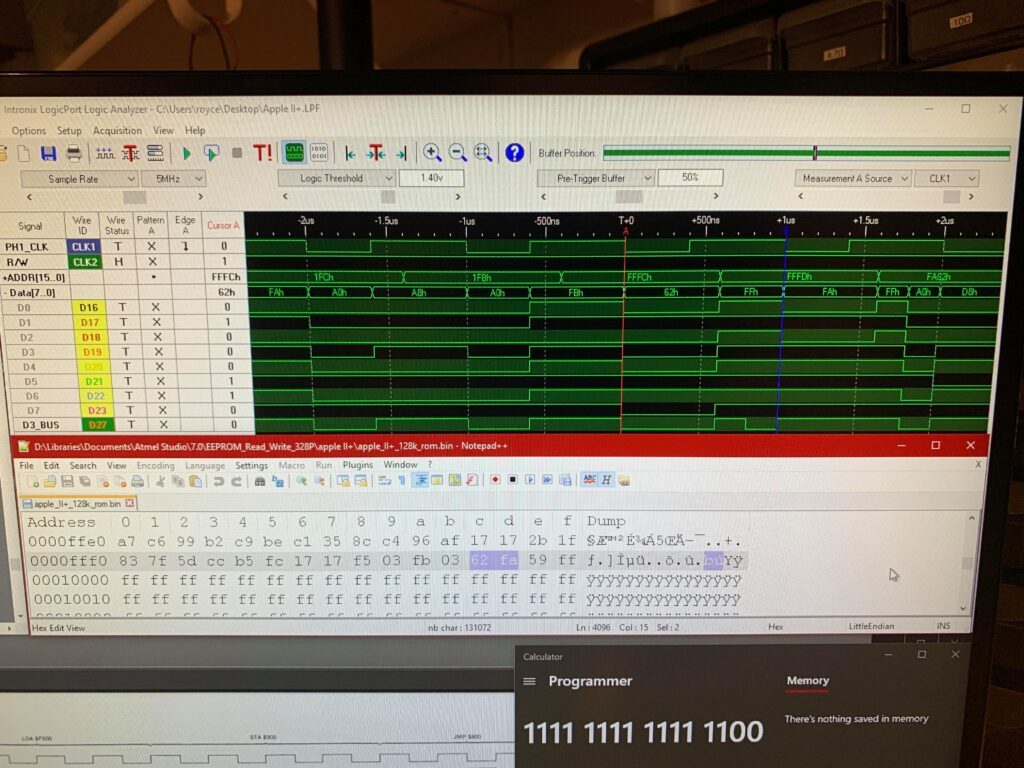
I set the logic analyzer software to trigger when the address bus = $FFFC (low byte of reset vector). It recorded that the CPU received $6A as the data at $FFFC. I compared that to the ROM file to see that the data should have been $62.
The next address the CPU output to the bus was $FFFD (high byte of reset vector). The CPU read $FA, which was correct according to the ROM file. The CPU followed up by outputting $FA6A on the address bus, which was evidence that the CPU was functioning correctly. Unfortunately, the data received by the CPU at $FA6A did not match the ROM file.
Eventually, I found a pattern that suggested data bus signal D3 was held HIGH whenever the ROM was accessed. I measured the D3 signal at the CPU with an oscilloscope scope, triggering on the ROM select signal, and found D3 floating in the 2-2.5V range. Then I placed the oscilloscope probe on the D3 output at the EEPROM and found that it changed state properly. Very strange… Confused, I checked for continuity between D3 at the EEPROM, the CPU, and each ROM IC socket. Aha! The D3 signal loses continuity between two of the ROM IC sockets!
Look carefully, and you can see the culprit:


The same blunt force trauma that broke the IC socket also took a chip out of the motherboard right along the D3 trace!
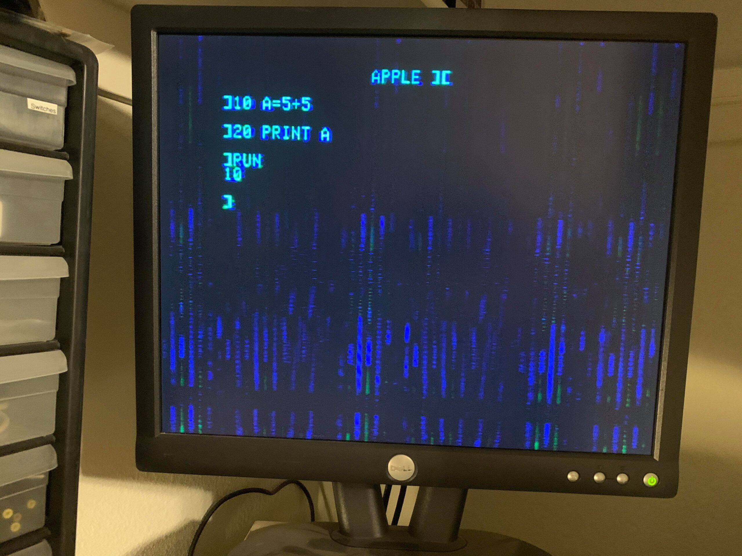
I added a jumper to the D3 pins between ROM IC sockets to bypass the trace damage, and I finally had a prompt!
Now that it had the correct reset vector data, the CPU could jump to the correct position in memory to begin the bootup sequence. You can see that here:
In the end, the actual problem with the system was minimal; it came down to a damaged trace. Although my improper power cycling caused the bridge rectifier to fail, it probably would have failed soon with normal usage. I could have saved myself some time by purchasing replacement ROM ICs or a 3rd party ROM card, but I was happy to experiment and learn from the experience!
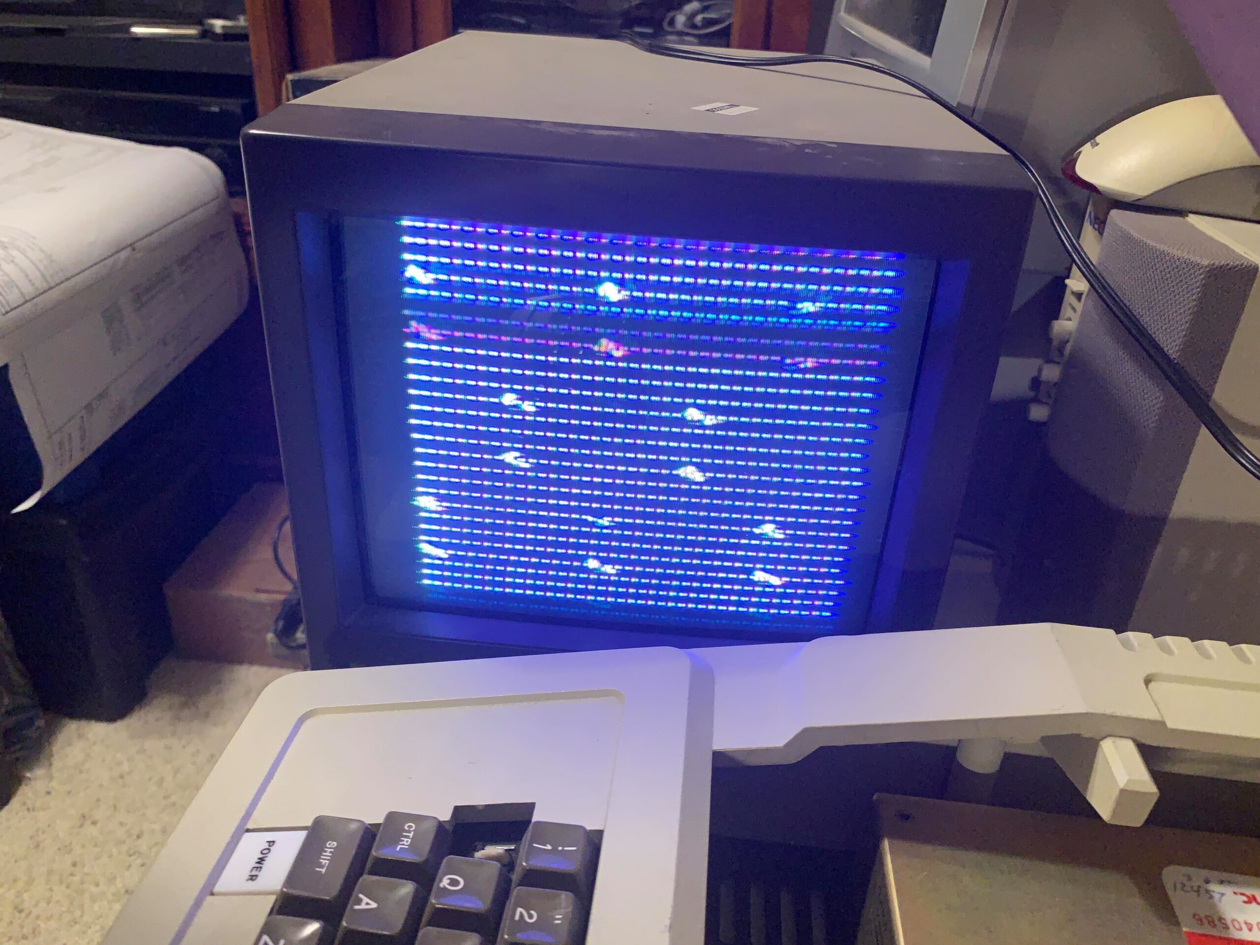
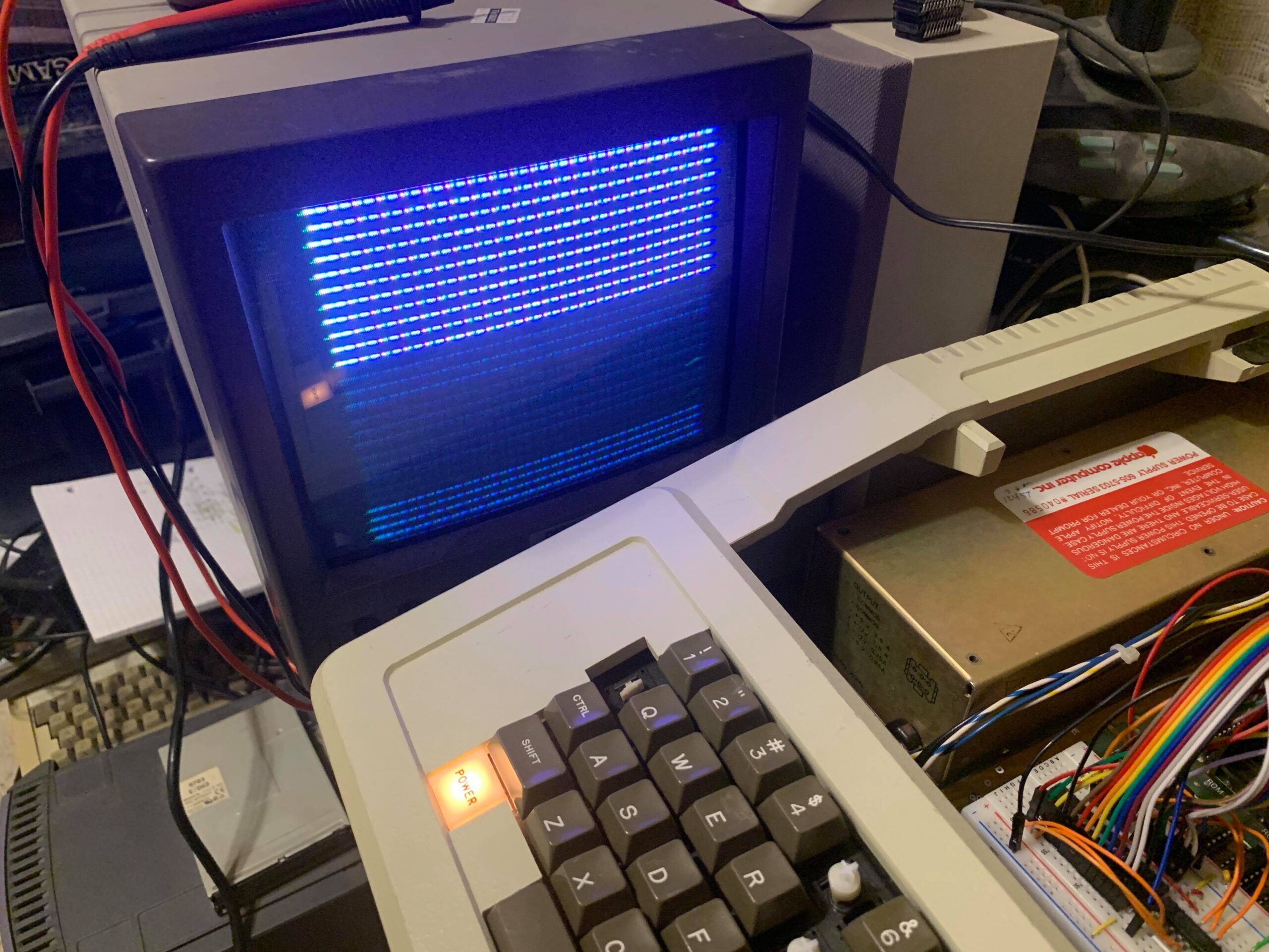
Here are some bonus pics of the system running a few games I found online. They were loaded into the system’s memory using its audio tape interface connected to a modern computer’s audio output.
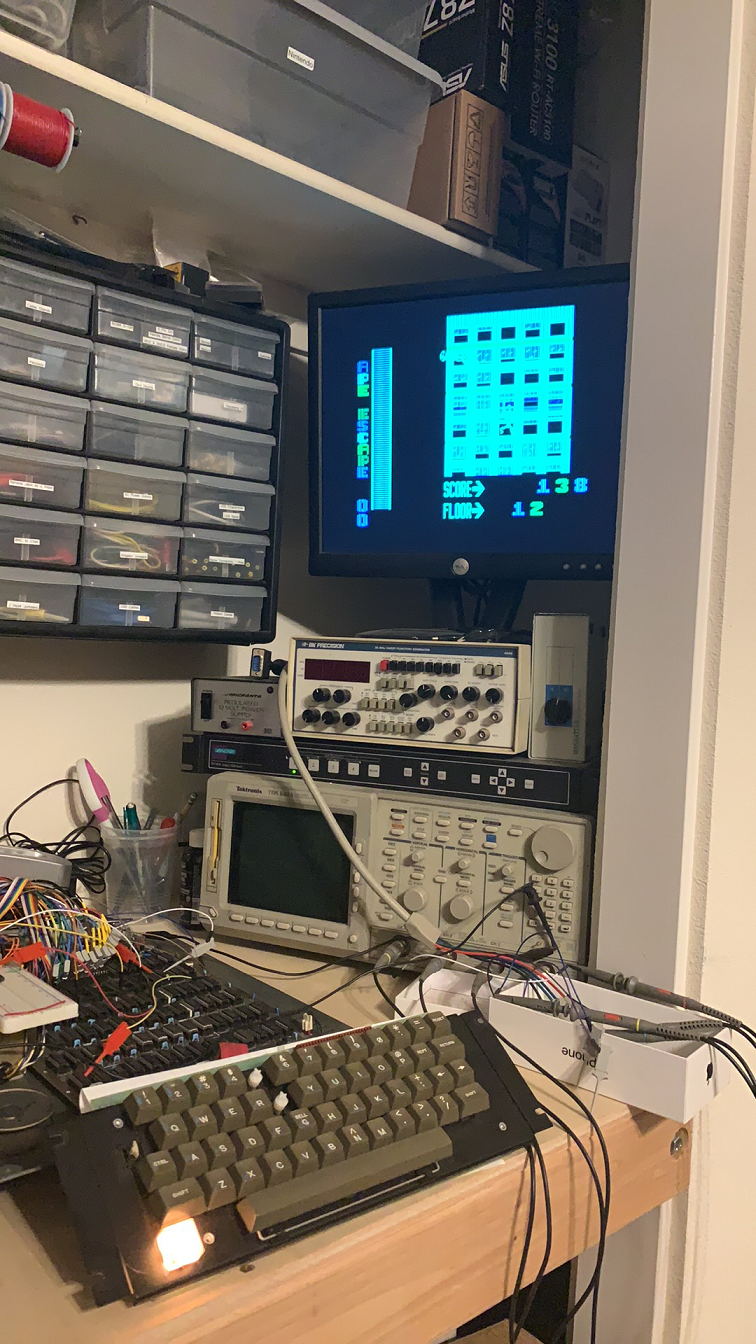


It looks much nicer with the replacement lid I purchased. Not pictured, I also picked up some keycaps to replace the missing ones. Only thing left to do now is order a 3D printed Alps short stem and 12° adapter to replace the damaged one for the escape key!