Asus P2B-D Dual Pentium iii-S 1.4 GHz Tualatin
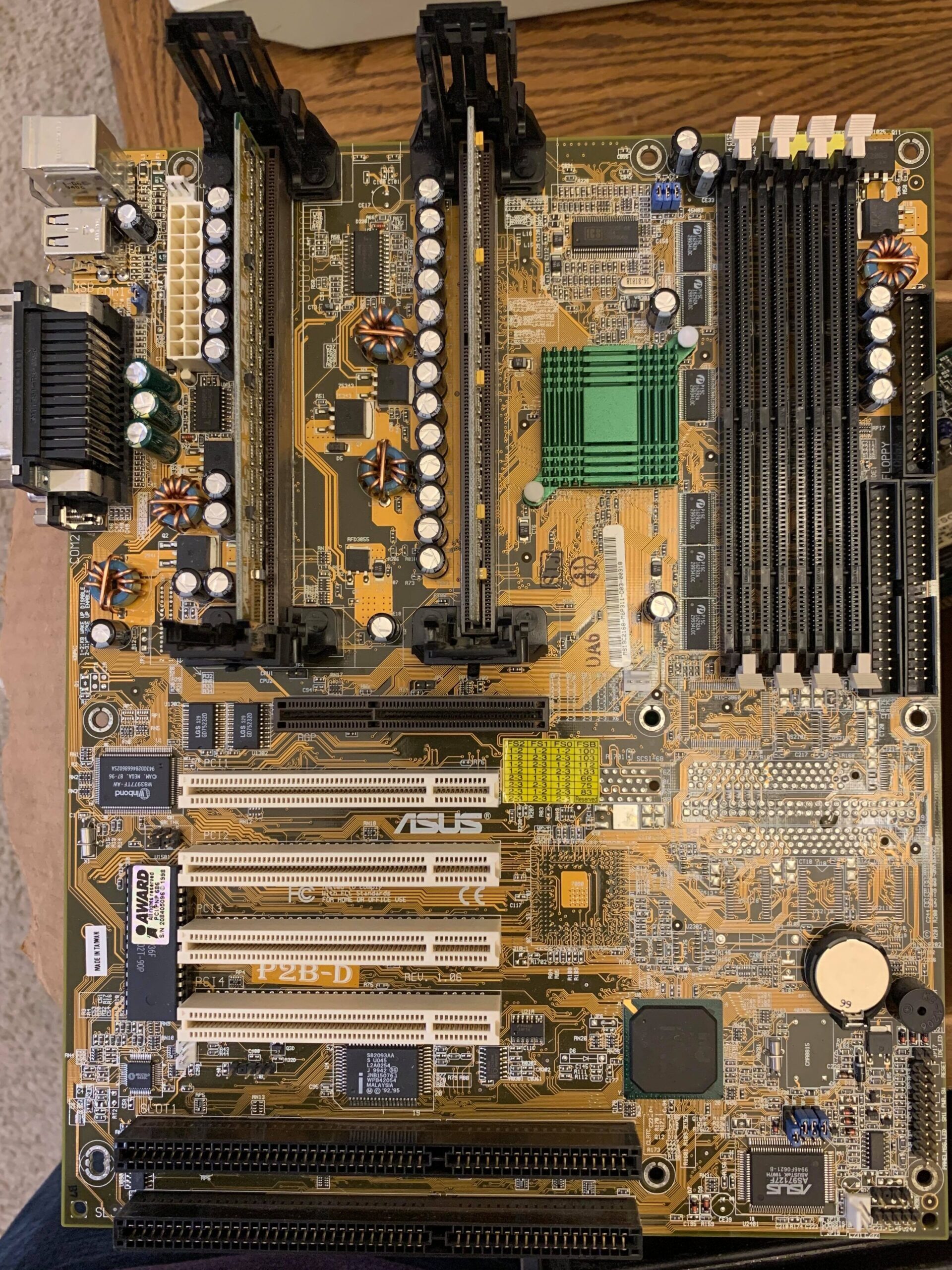
I came across a listing for this Asus P2B-D and I immediately knew that it would make for a fun project.
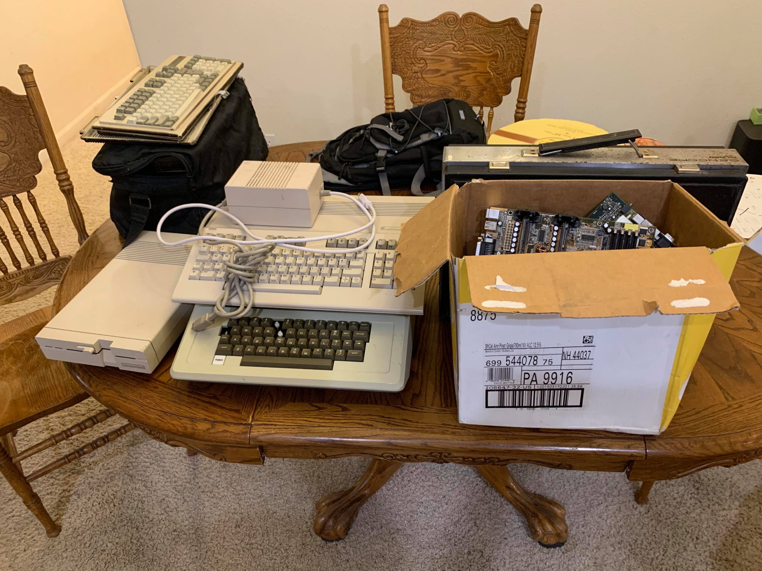
As an aside: after driving an hour to pick this board up, I ended up buying an entire lot of vintage hardware which will be covered in various future posts. Here’s a preview of the lot:
The P2B-D/DS motherboards produced by Asus consist of the Intel 440BX chipset and dual slot 1 CPU connectors with support for Pentium 2 & 3 processors. With board revision 1.06 came support for Coppermine-based CPUs.
I found a treasure trove of information for modifying the Asus P2B boards at http://tipperlinne.com/p2bmod.html [archive.org link]. Because these modifications are so well documented on that page, I won’t be going into details here.
I was able to procure this in-box (with manual!) Asus S370-DL Revision 1.02 slot 1 to socket 370 adapter, AKA slocket:
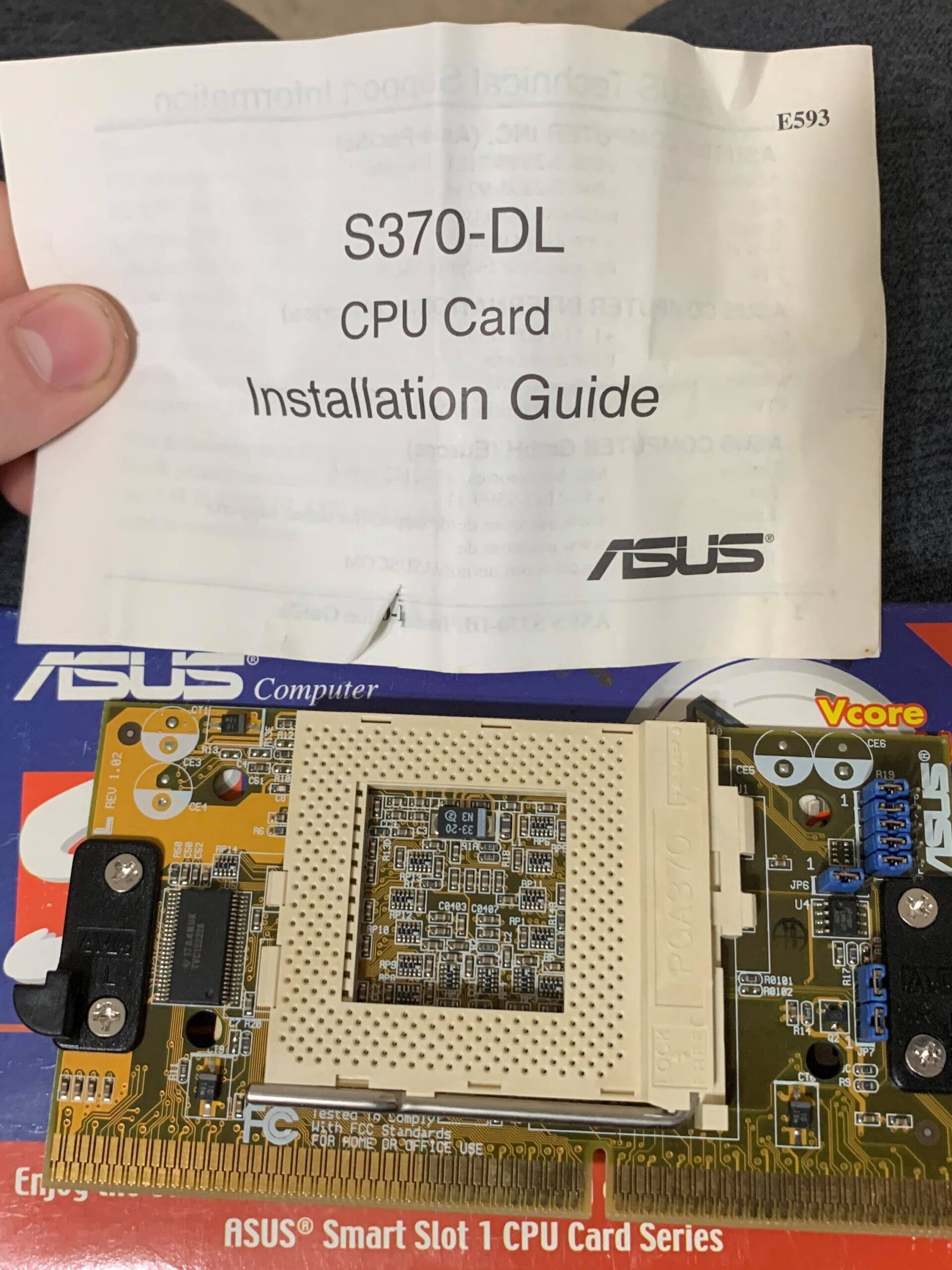
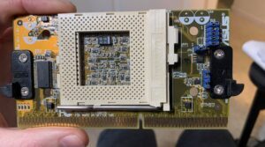
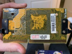
For this slocket to accept the Tualatin Pentium iii-S, it had to be modified by removing a couple of pins and adding a jumper wire to relocate another pin.
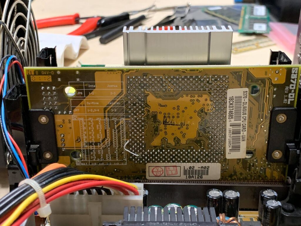
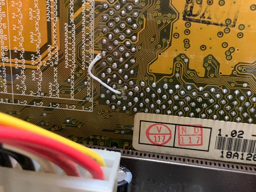
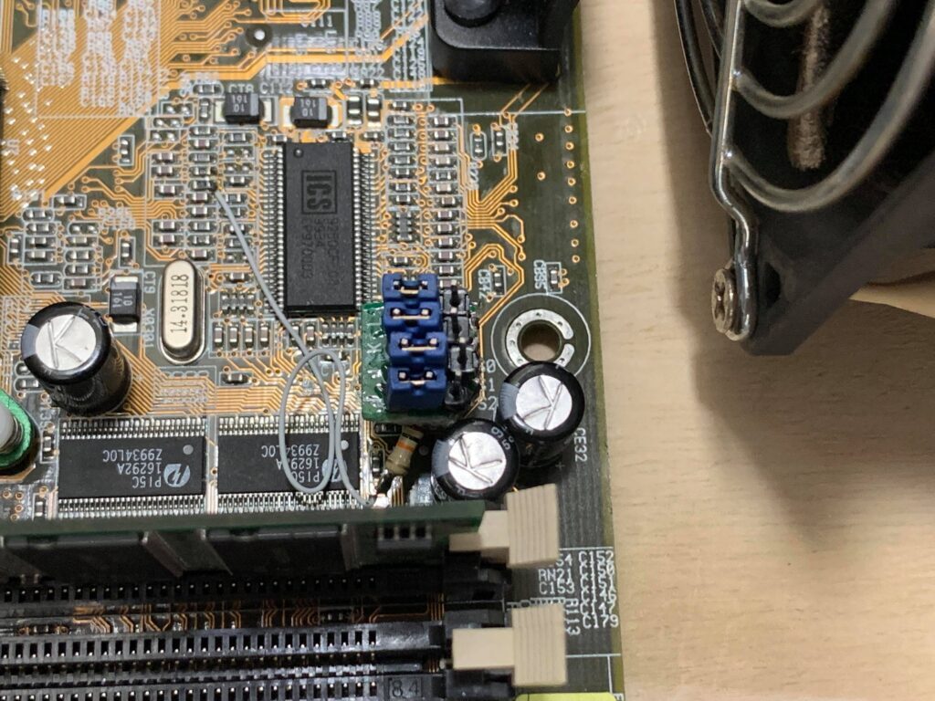
There were a multitude of modifications made to the motherboard to enable unofficial support for the Tualatin Pentium iii-S, beginning with the addition of another FSB frequency jumper. The existing FSB clock generator supports a fourth frequency select jumper that Asus didn’t include in their design. According to the sticker on the motherboard an FSB of 133 MHz is possible, but that particular setting also inadvertently overclocks the PCI bus. With the addition of the fourth FSB jumper, 133 MHz can be selected without overlocking the PCI bus, however the AGP bus will also become overclocked (of which ATI AGP video cards are apparently sensitive but nVidia cards not as much).
I made this little jumper pack that connects right on top of the original three jumpers and adds the fourth jumper:

That was the minimum just to get the board to POST with the Tualatin CPU.
I wish I had taken pictures of the other mods, but they are all very well spelled out on the tipperlinne link. The purpose of the rest of the modifications were to:
1. Reduce Vtt (signal voltage) to increase stability and prolong CPU life
2. Increase Vio (RAM voltage) for better stability with 133 MHz memory modules
3. Add Tualatin tB1 stepping microcode to the P2B BIOS
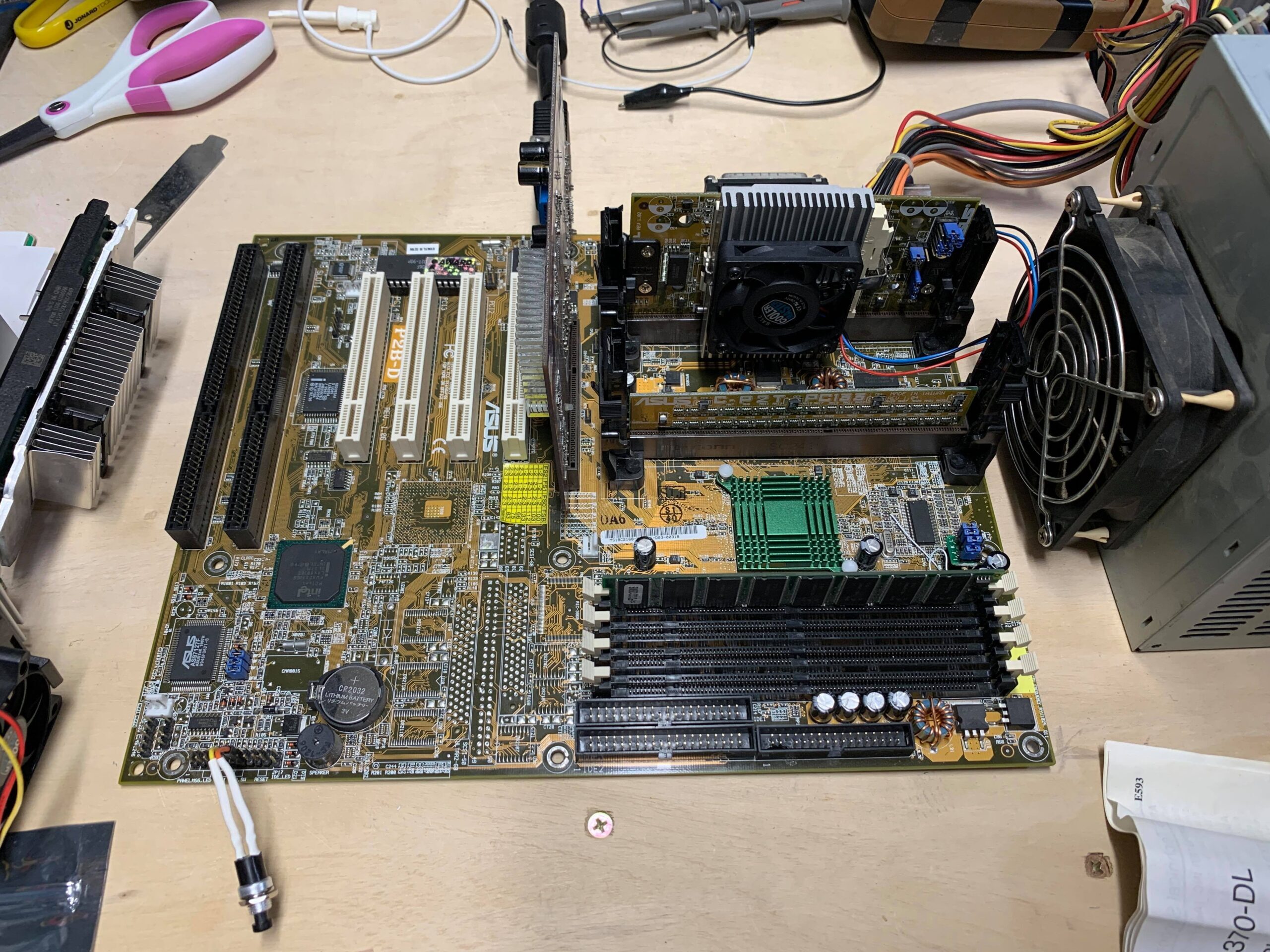
Here’s the complete board (I’ve since acquired 1GB worth of 256MB 133 MHz memory):


Leave a Reply
You must be logged in to post a comment.